Introduction
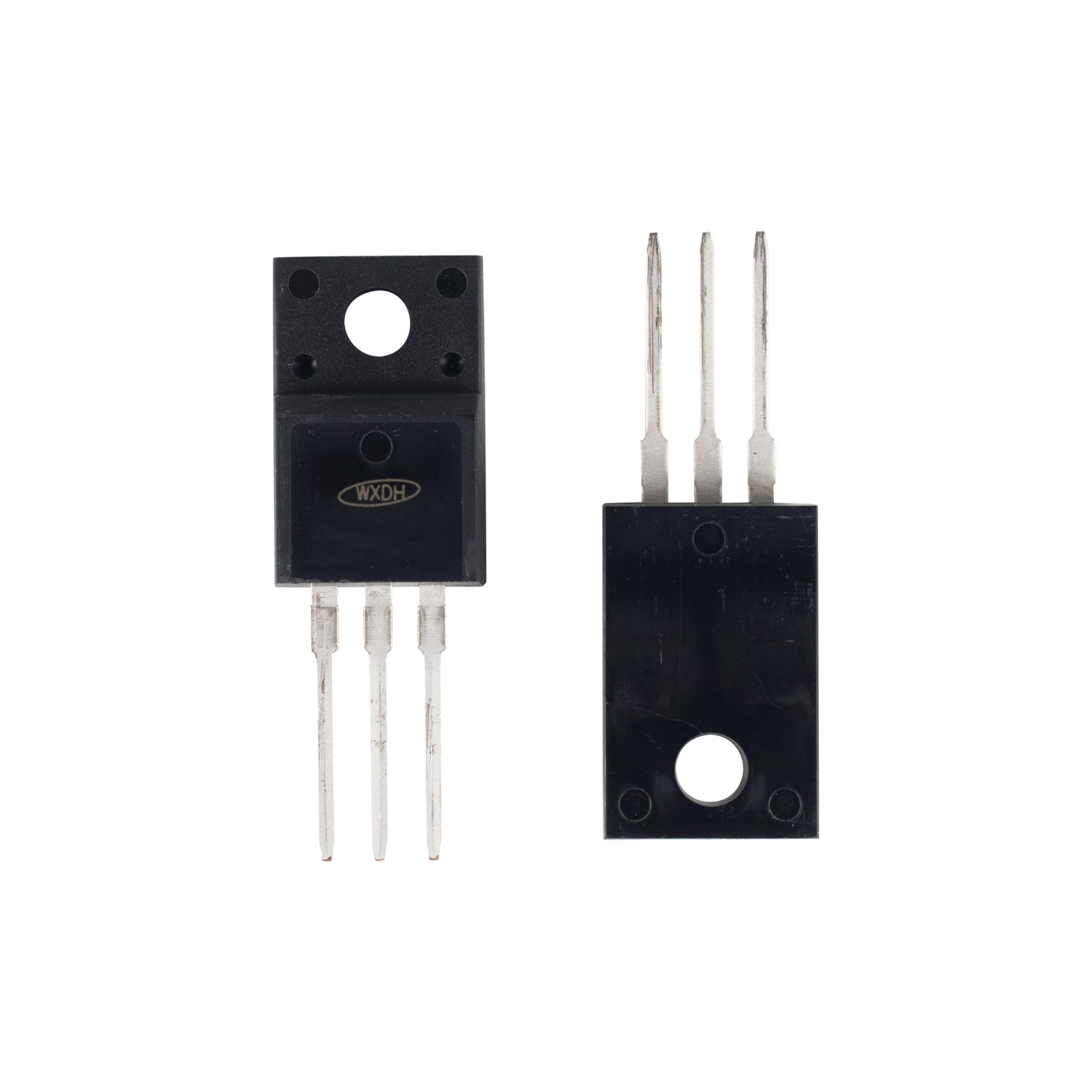
Enhancement-mode MOSFETs are pivotal components in modern electronics, particularly in digital circuits and power management systems. As transistors that operate with no current flowing when zero voltage is applied, they have become integral in designing efficient and high-performance electronic devices. This article delves into the intricacies of enhancement-mode MOSFETs, exploring their operation principles, applications, and advantages. Understanding these devices is essential for professionals aiming to optimize circuits for better performance and energy efficiency. For a deeper insight into practical implementations, exploring Enhancement Mode Power devices can be highly beneficial.
Fundamentals of Enhancement-mode MOSFETs
Enhancement-mode MOSFETs are a type of field-effect transistor (FET) that requires a gate-source voltage to induce a conductive channel between the drain and source terminals. Unlike depletion-mode MOSFETs, which conduct at zero gate voltage, enhancement-mode devices are normally off when no voltage is applied. This characteristic makes them ideal for use as voltage-controlled switches in various electronic applications.
The operation of enhancement-mode MOSFETs is based on the modulation of charge carriers in a semiconductor channel. When a positive gate voltage is applied in an N-channel device, it attracts electrons towards the gate oxide layer, forming a conductive channel. This allows current to flow between the drain and source terminals. The threshold voltage is a critical parameter, indicating the minimum gate voltage required to form this channel.
N-Channel vs. P-Channel Enhancement-mode MOSFETs
Enhancement-mode MOSFETs come in two primary types: N-channel and P-channel. N-channel MOSFETs use electrons as charge carriers and require a positive gate voltage relative to the source. P-channel MOSFETs, on the other hand, use holes as charge carriers and require a negative gate voltage. N-channel devices typically offer better performance characteristics, such as lower on-resistance and higher electron mobility, making them more prevalent in high-speed applications.
Operation Principles
The operation of an enhancement-mode MOSFET centers around the electric field effect. When a voltage is applied to the gate terminal, it creates an electric field that influences the conductivity of the channel. The gate is insulated from the channel by a thin layer of silicon dioxide, which acts as a dielectric. This insulation allows the gate to control the channel conductivity without direct current flow, resulting in high input impedance.
The drain current in an enhancement-mode MOSFET can be controlled precisely by adjusting the gate voltage. This capability is essential for amplification and switching applications. The device operates in different regions depending on the gate voltage and drain-source voltage, including the cut-off region, triode region, and saturation region. Understanding these regions is crucial for designing circuits that leverage the full potential of the MOSFET.
Threshold Voltage and Its Importance
The threshold voltage (Vth) is a key parameter in enhancement-mode MOSFETs. It defines the minimum gate-to-source voltage required to create a conductive channel. Factors affecting the threshold voltage include the doping concentration of the substrate, the thickness of the oxide layer, and the work function difference between the gate material and the substrate. Precise control over Vth is essential for ensuring that the MOSFET operates correctly within a circuit, particularly in digital logic applications where voltage levels represent binary states.
Applications of Enhancement-mode MOSFETs
Enhancement-mode MOSFETs are widely used in various electronic applications due to their efficient switching characteristics and high input impedance. They are fundamental components in digital integrated circuits, such as microprocessors and memory devices, where they function as logic switches. Their ability to operate at low power levels makes them ideal for battery-powered devices and portable electronics.
In power electronics, enhancement-mode MOSFETs serve as high-speed switches in power converters and inverters. Their fast switching speeds and low on-resistance contribute to higher efficiency in power management systems. Additionally, they are used in analog circuits for amplification purposes, leveraging their linear region of operation for signal processing applications.
Use in Power Management Systems
In power management, enhancement-mode MOSFETs play a critical role in voltage regulation and power conversion. They are used in DC-DC converters, where they switch rapidly to control the output voltage and current, improving the overall efficiency of the power supply. Their capacity to handle high voltages and currents while maintaining low power loss is essential for modern power systems.
For applications requiring high reliability and efficiency, such as in renewable energy systems and electric vehicles, exploring advanced Enhancement Mode Power MOSFETs offers significant advantages. These devices are designed to withstand harsh operating conditions while delivering optimal performance.
Advantages of Enhancement-mode MOSFETs
Enhancement-mode MOSFETs offer several benefits that make them preferable in many electronic designs. Their high input impedance means they draw minimal gate current, reducing power consumption and preventing loading of preceding circuit stages. This characteristic is particularly advantageous in amplifier circuits and signal processing applications.
Another advantage is their fast switching capability. Enhancement-mode MOSFETs can transition between on and off states rapidly, which is crucial in high-frequency applications and switching power supplies. Their low on-resistance reduces power losses during conduction, improving the efficiency of power converters and inverters.
Thermal Performance and Reliability
Thermal performance is a critical aspect of semiconductor devices. Enhancement-mode MOSFETs typically exhibit good thermal stability, which enhances their reliability in various operating conditions. Proper thermal management ensures that the device operates within safe temperature limits, prolonging its lifespan and maintaining consistent performance.
The robust construction of these MOSFETs allows them to handle significant power levels. By selecting devices from reputable sources, such as specialized Enhancement Mode Power MOSFETs, designers can ensure high reliability and efficiency in their applications.
Design Considerations
When incorporating enhancement-mode MOSFETs into a design, several factors must be considered to optimize performance. These include the selection of appropriate gate drive voltage, understanding the switching characteristics, and managing parasitic elements such as capacitance and inductance that can affect switching performance.
Gate drive circuitry needs to provide adequate voltage levels to fully turn on the MOSFET, ensuring low on-resistance and minimizing conduction losses. Additionally, the gate drive must be able to switch the MOSFET rapidly to reduce switching losses, which is especially important in high-frequency applications.
Parasitic Capacitance and Inductance
Parasitic capacitance between the gate, drain, and source can impact the switching speed of the MOSFET. High parasitic capacitance requires more energy and time to charge and discharge during switching events, which can slow down the device and increase losses. Minimizing these parasitic elements through careful PCB layout and component selection is crucial.
Parasitic inductance, often arising from circuit traces and component leads, can cause voltage spikes during switching due to the inductive kickback effect. These voltage spikes can potentially exceed the maximum ratings of the MOSFET, leading to device failure. Implementing snubber circuits and using layout techniques to reduce inductance can mitigate these risks.
Latest Developments in MOSFET Technology
Advancements in semiconductor technology have led to significant improvements in MOSFET performance. The development of silicon carbide (SiC) and gallium nitride (GaN) MOSFETs has introduced devices with superior electrical characteristics, such as higher breakdown voltages and faster switching speeds. These devices are expanding the application possibilities for MOSFETs in high-power and high-frequency domains.
Moreover, the integration of enhancement-mode MOSFETs into intelligent power modules (IPMs) and system-in-package (SiP) solutions is enhancing the efficiency and compactness of electronic systems. For instance, devices available at Enhancement Mode Power modules offer integrated solutions for complex power management challenges.
Impact on Renewable Energy and Automotive Applications
In renewable energy systems, such as solar inverters and wind turbines, enhancement-mode MOSFETs contribute to efficient energy conversion and management. Their ability to handle high voltages and currents with minimal losses is crucial for maximizing energy harvest and reducing operational costs.
In the automotive industry, the shift towards electric vehicles (EVs) has increased the demand for high-efficiency power electronics. Enhancement-mode MOSFETs are integral in EV powertrain systems, battery management, and charging infrastructure. Their performance directly affects the vehicle's efficiency, range, and reliability.
Comparing Enhancement-mode and Depletion-mode MOSFETs
While enhancement-mode MOSFETs are normally off without gate voltage, depletion-mode MOSFETs are normally on. This fundamental difference affects how they are used in circuits. Enhancement-mode devices are preferred for applications requiring devices to be off at zero gate voltage, providing fail-safe conditions in power circuits.
Depletion-mode MOSFETs find niche applications where a normally-on device is desirable. However, they are less common due to the safety and control advantages offered by enhancement-mode devices. Making an informed choice between these types depends on the specific requirements of the application.
Practical Implications in Circuit Design
In circuit design, enhancement-mode MOSFETs provide greater control and are easier to interface with logic-level signals. They do not conduct unless activated, reducing the risk of unintended current flow. This characteristic simplifies the design of standby power systems and contributes to overall energy savings.
For engineers looking to integrate these devices, resources such as Enhancement Mode Power components provide a wide selection of MOSFETs tailored for various applications, ensuring that the optimal device is available for any design challenge.
Future Trends
The future of enhancement-mode MOSFETs is poised for growth, driven by the increasing demand for efficient power electronics. Ongoing research focuses on improving material properties, such as developing new semiconductor materials with higher electron mobility and thermal conductivity. These advancements aim to enhance performance while reducing device size and cost.
Integration with digital control systems is another trend, enabling smarter power management solutions. The combination of enhancement-mode MOSFETs with microcontrollers and digital signal processors facilitates the development of adaptive systems that can optimize performance in real-time.
Impact of Emerging Technologies
Emerging technologies such as the Internet of Things (IoT) and Industry 4.0 are increasing the demand for energy-efficient and compact power solutions. Enhancement-mode MOSFETs are at the forefront of meeting these needs, and their evolution will significantly influence the effectiveness of future electronic systems.
Companies providing cutting-edge Enhancement Mode Power MOSFETs are essential partners in this technological progression, offering components that meet the stringent requirements of next-generation applications.
Conclusion
Enhancement-mode MOSFETs are indispensable in modern electronics, offering superior control and efficiency for a wide range of applications. Their ability to operate as voltage-controlled switches with high input impedance makes them ideal for both digital and analog circuits. As technology advances, these devices continue to evolve, providing even greater performance and efficiency.
Understanding the principles and operational nuances of enhancement-mode MOSFETs is crucial for engineers and professionals in the field. Leveraging resources and products from industry leaders in Enhancement Mode Power devices ensures access to the latest advancements and highest quality components, enabling the development of innovative and efficient electronic systems.


