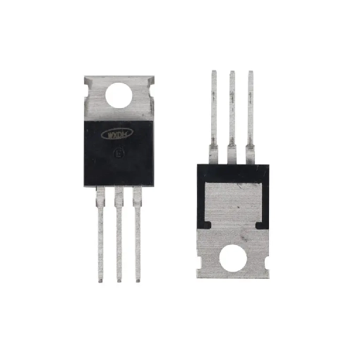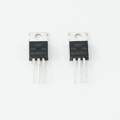
Understanding the Importance of MOSFETs in Modern Electronics
The Metal–Oxide–Semiconductor Field-Effect Transistor (MOSFET) is one of the most critical components in modern electronic systems. It lies at the core of nearly every digital and power control circuit—from smartphones and laptops to electric vehicles, renewable energy inverters, and industrial automation systems.
Engineers often describe the MOSFET as the “heart of power electronics”, thanks to its efficiency, speed, and ability to switch or amplify electrical signals with minimal energy loss. Understanding its working principle is fundamental for anyone involved in electronics design or research.
So, what is the working principle of a MOSFET? In simple terms, a MOSFET operates as a voltage-controlled switch or amplifier that controls the flow of current between two terminals—the source and the drain—by applying a voltage at the gate terminal. Its unique structure and operation make it superior to traditional transistors in terms of switching speed, efficiency, and scalability.
This article explores the structure, operating modes, and behavior of MOSFETs, breaking down how they work, how they control current, and why they are essential in both analog and digital circuits.
Structure of a MOSFET
1. Basic MOSFET Terminals
AMOSFET has four terminals that play distinct roles in its operation:
Terminal | Symbol | Function |
Gate | G | Controls the flow of current by creating an electric field |
Source | S | Entry point for charge carriers (electrons or holes) |
Drain | D | Exit point for charge carriers |
Body/Substrate | B | The underlying semiconductor material that influences device behavior |
The gate is separated from the channel by a thin insulating oxide layer, usually made of silicon dioxide (SiO₂). This insulation prevents direct current flow into the gate, giving MOSFETs extremely high input impedance—one of their most desirable features.
2. N-Channel vs. P-Channel MOSFETs
MOSFETs come in two major types based on their semiconductor channel:
Type | Charge Carriers | Gate Voltage Required for Conduction | Common Use |
N-Channel | Electrons (negative charge) | Positive gate voltage relative to source | Power electronics, high-speed switching |
P-Channel | Holes (positive charge) | Negative gate voltage relative to source | Low-side switching, complementary circuits |
N-channel MOSFETs are generally faster and more efficient because electrons move more quickly than holes, resulting in lower resistance and higher conductivity.
3. Enhancement vs. Depletion Mode MOSFETs
MOSFETs are further classified by their mode of operation:
Mode | Default State (No Gate Voltage) | Behavior | Common Usage |
Enhancement | OFF | Requires gate voltage to create channel | Switching applications |
Depletion | ON | Gate voltage reduces channel conductivity | Analog circuits, biasing networks |
Most MOSFETs used in modern electronics are enhancement-mode, meaning they require a gate-to-source voltage (Vgs) to turn on.
Key Electrical Parameters of a MOSFET
Understanding a MOSFET’s working principle involves analyzing its electrical characteristics, which determine how it responds to voltage and current.
Parameter | Description | Importance |
Threshold Voltage (Vth) | Minimum gate voltage required to form a conductive channel | Defines ON/OFF behavior |
Drain–Source Resistance (Rds(on)) | Resistance when MOSFET is ON | Determines conduction losses |
Gate Capacitance (Cg) | Capacitance between gate and channel | Affects switching speed |
Transconductance (gm) | Change in drain current per change in gate voltage | Measures amplification ability |
Breakdown Voltage (Vds(max)) | Maximum voltage before damage | Defines safe operating limits |
Each of these parameters directly influences how efficiently and reliably a MOSFET operates in real-world circuits.
Working Principle of a MOSFET
The working principle of a MOSFET is based on electrostatic control. The voltage applied at the gate terminal modulates the conductivity of the channel between the source and drain, allowing or preventing current flow.
1. How Voltage Controls Current
When no voltage is applied to the gate, the MOSFET remains OFF because there is no conductive path between the source and drain.
When a sufficient voltage (Vgs) is applied, an electric field forms across the oxide layer.
This field attracts charge carriers (electrons in N-channel, holes in P-channel), forming a conductive channel between the source and drain.
Current begins to flow once the drain-to-source voltage (Vds) is applied.
Thus, the gate voltage electrostatically “opens” or “closes” the channel, allowing precise control of current flow.
2. The Role of the Oxide Layer
The thin oxide layer between the gate and channel acts as an insulator. Because of this:
The gate draws almost no current, making MOSFETs energy-efficient.
Small voltage changes at the gate can control large currents at the drain, giving the device excellent gain and switching properties.
3. Carrier Flow and Channel Formation
In an N-channel enhancement MOSFET, a positive gate voltage attracts electrons to the channel region, forming an inversion layer that connects the source and drain.
In contrast, in a P-channel device, a negative gate voltage attracts holes to form the conduction channel.
This field-controlled formation of a conductive path is what makes MOSFETs distinct from other transistors.

Operating Modes of MOSFET
MOSFETs operate in three major regions, each representing a unique electrical behavior:
1. Cutoff Region
Gate voltage < Threshold voltage (Vgs < Vth)
No channel forms, so the MOSFET is OFF
Used in switching applications where current blocking is required.
2. Triode (Linear) Region
Vgs > Vth and Vds is small
Channel behaves like a variable resistor
Ideal for analog control and amplification
3. Saturation (Active) Region
Vgs > Vth and Vds is large
Channel is fully formed, current saturates
Used in switching applications where MOSFET is fully ON
Mode | Condition | MOSFET Behavior | Common Application |
Cutoff | Vgs < Vth | OFF (No conduction) | Isolation, protection |
Linear | Vgs > Vth and low Vds | Acts as variable resistor | Amplification |
Saturation | Vgs > Vth and high Vds | Fully ON | Switching, power control |
Switching Behavior of MOSFETs
MOSFETs are known for their high-speed switching capabilities, which make them essential in power conversion, digital logic, and pulse-width modulation (PWM) circuits.
1. Turning ON and OFF
Turn ON: Gate voltage exceeds Vth, creating a conductive channel.
Turn OFF: Gate voltage drops below Vth, collapsing the channel and stopping current.
Switching speed depends on:
Gate charge (Qg)
Gate resistance (Rg)
Driver strength
Faster switching minimizes power loss but can introduce electromagnetic interference (EMI) if not properly managed.
2. Switching Losses
Switching losses occur during transition periods when both voltage and current overlap. To reduce these:
Use low gate charge MOSFETs
Optimize gate driver design
Reduce parasitic capacitances
MOSFETs in AC and DC Applications
MOSFETs are versatile devices used in both DC and AC circuits. Their function changes slightly depending on the nature of the current.
1. MOSFETs in DC Circuits
Function primarily as electronic switches.
Control steady voltage or current.
Common in DC–DC converters, battery management systems, and motor drivers.
2. MOSFETs in AC Circuits
Operate in linear mode to amplify or modulate alternating signals.
Used in audio amplifiers, RF circuits, and communication equipment.
Control waveform amplitude and frequency response.
Comparison | DC Operation | AC Operation |
Function | Switch | Amplifier/Modulator |
Current Type | Constant | Alternating |
Primary Control | ON/OFF | Linear variation |
Application | Converters, power control | Signal processing, communication |
Factors Affecting MOSFET Performance
1. Temperature Effects
Rising temperature increases resistance (Rds(on)).
Threshold voltage decreases, leading to higher leakage current.
2. Parasitic Capacitances
Gate–source and gate–drain capacitances slow down high-speed operation.
Must be minimized for high-frequency switching.
3. Gate Drive Requirements
The driver circuit must provide sufficient current to charge/discharge the gate capacitance quickly.
Proper driver selection improves efficiency and reliability.
4. Thermal Management
Use of heat sinks or MOSFET packages ensures stable operation under high load.
Modern Trends in MOSFET Design
1. Wide Bandgap MOSFETs
SiC (Silicon Carbide) and GaN (Gallium Nitride) technologies are transforming the power electronics landscape.
Offer higher breakdown voltage, lower losses, and faster switching than silicon.
2. Smart Power Integration
Integration of MOSFETs with control ICs for improved power efficiency.
Used in EV chargers, renewable energy systems, and advanced communication devices.
3. Nano-scale MOSFETs
Found in modern CPUs and microcontrollers.
Enable billions of transistors per chip with extremely low power consumption.
Conclusion
In essence, the working principle of a MOSFET revolves around voltage-controlled conductivity. By applying voltage to the gate, an electric field forms that regulates current between the source and drain. This simple yet powerful principle enables MOSFETs to function as both high-speed switches and linear amplifiers across a vast range of applications.
From power control in DC systems to signal amplification in AC circuits, MOSFETs have become the foundation of efficient electronic design. As technology advances toward smarter, faster, and greener solutions, MOSFET innovation continues to shape the future of electronics.
For high-performance, reliable, and energy-efficient MOSFET solutions, Jiangsu Donghai Semiconductor Co., Ltd. stands as a trusted partner—delivering advanced semiconductor products built for precision, durability, and modern application needs.
FAQs
Q1: What is the basic working principle of a MOSFET?
A: A MOSFET works by using an electric field to control the flow of current between the source and drain, based on the gate voltage applied.
Q2: Why is MOSFET called a voltage-controlled device?
A: Because the gate voltage, not gate current, determines whether the MOSFET is ON or OFF.
Q3: What are the main operating regions of a MOSFET?
A: Cutoff (OFF), Triode/Linear (Variable resistance), and Saturation (Fully ON).
Q4: What is the difference between N-channel and P-channel MOSFETs?
A: N-channel MOSFETs use electrons as carriers and need positive gate voltage, while P-channel uses holes and needs negative gate voltage.
Q5: What role does the oxide layer play in MOSFET operation?
A: It acts as an insulator, allowing the gate to control current flow without drawing current itself.
Q6: Can a MOSFET be used in both AC and DC circuits?
A: Yes, MOSFETs can efficiently switch DC power or amplify AC signals, depending on the design.
Q7: What factors affect MOSFET performance?
A: Temperature, gate capacitance, switching speed, and thermal management all influence MOSFET efficiency.


